20.08.2024
The quantum chip visualization we finally liked

20.08.2024

In Part 1 and Part 2 of our qubit visualizations journey, we explored different concepts and created a few short, okay-ish films. Only to realize that we needed a far more powerful computer and better storytelling skills to actually bring our vision to life.
As we waited for the computer parts to arrive and learned the basics of cinematography, we got the chance to completely rethink our approach to qubit visualization.
All our previous concepts relied on abstract representations, like Bloch spheres or probability distributions, rather than direct observation. This time, however, we asked ourselves: why not move from the abstract closer to the physical? What if we looked at it under a microscope?
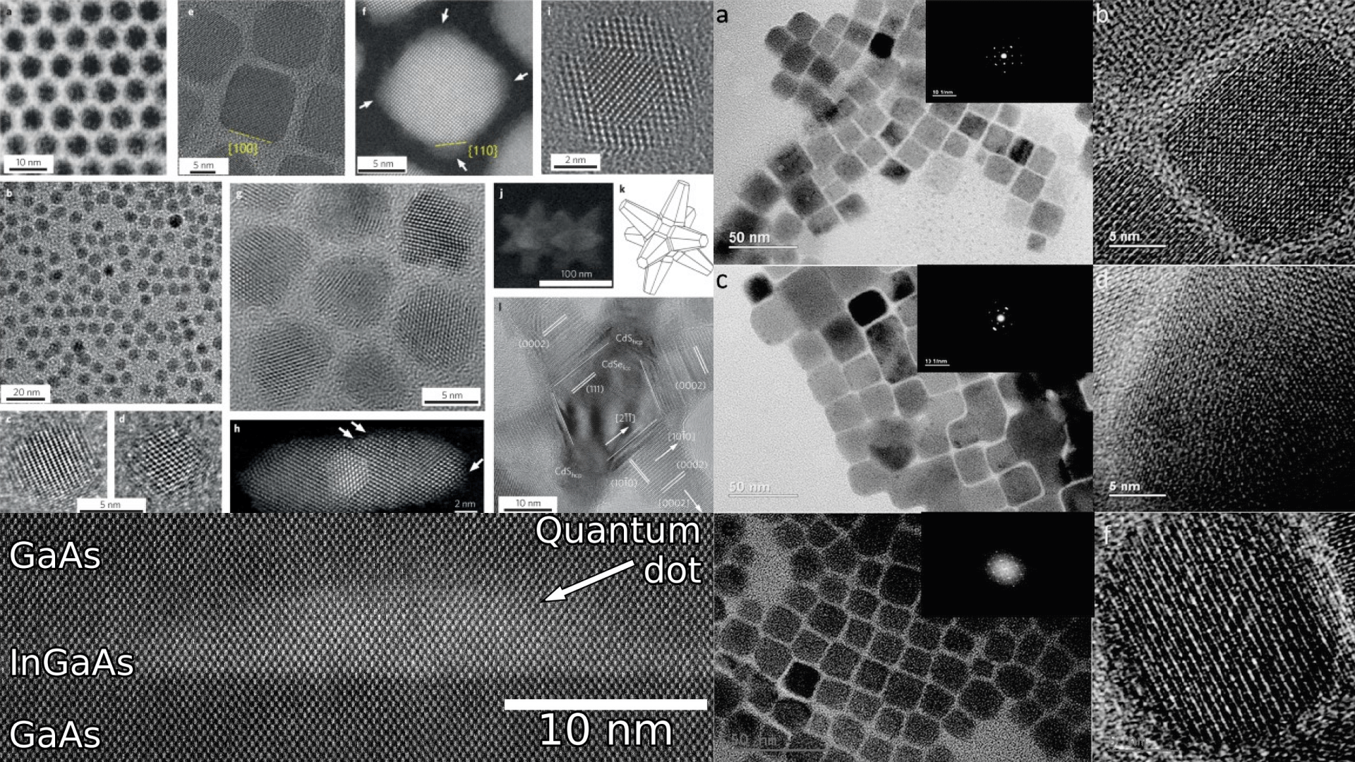
A quantum bit itself isn’t something you can directly observe under a microscope, but the physical structures used to implement qubits can be seen with specialized equipment. For example, superconducting qubits, which we visualized in previous blog posts, are typically implemented using tiny circuits made of superconducting materials like aluminum or silicon. With an electron microscope, you can observe the patterns of these circuits.

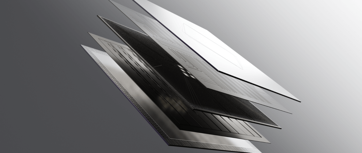
These under-the-microscope photos inspired us to develop a new concept: visualizing the qubit as a reflection on a surface. The reflection is constantly changing, but you can capture its state by taking a photo. It’s not tangible, but it’s there—just like a qubit.
With the concept for the quantum bit in place, we began working on the film’s storytelling, which had been a challenge in previous posts.
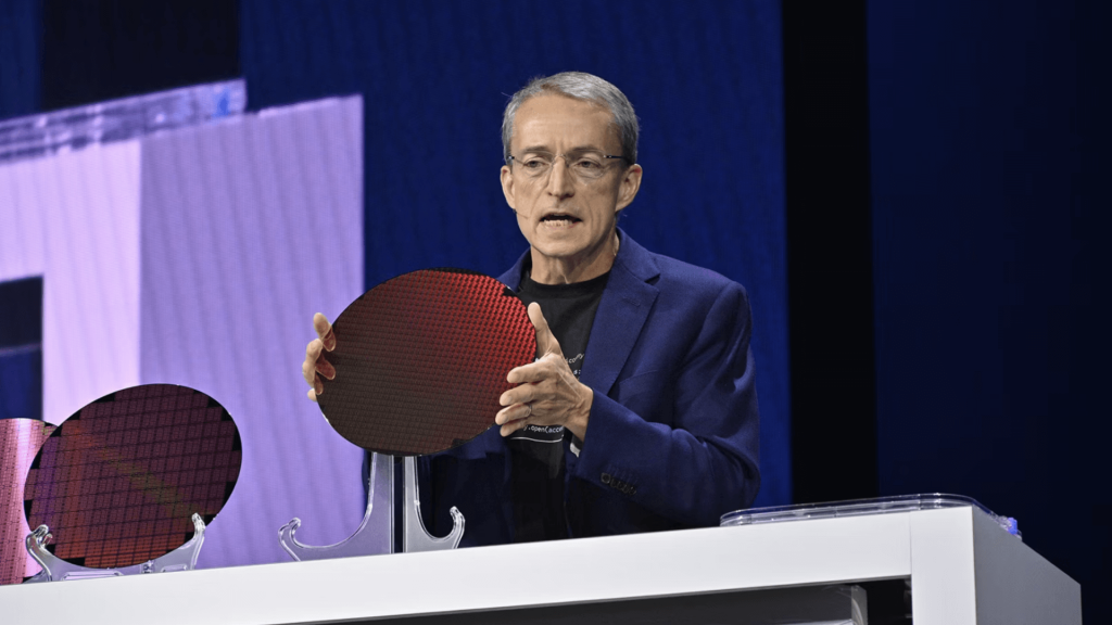
First, to make the story more complete, we decided to add an important element to the film—the semiconductor wafer. A wafer is a thin, flat disc made of semiconductor material on which chips are fabricated. Although the chip is the end result of wafer processing—cut from the wafer, tested, and packaged—the wafer itself looks much more impressive and better showcases advanced technology compared to individual chips. That’s why quantum companies that use wafers in manufacturing often feature them in their marketing instead of chips.

Second, we needed to solve the scalability problem that we struggled with in previous parts. It was difficult to recognize the qubit as it scaled from a larger size to a smaller one within the chip, and introducing the wafer only compounded this issue.
To address this, we decided to tell the entire story within a single object—a round disk surface—and structure the animation to flow from the smallest element to the largest: starting with one qubit, moving to a qubit cluster, then to a chip, followed by a chip array, and finishing with the wafer.
With this approach, realistic sizes became less critical since all elements would be shown on a single surface.
This approach defined our composition: the primary animation will illustrate the transition from a single qubit to the wafer within the object, while the secondary animation will focus on the movement of the object and transitions between scenes.
As we got the story and transitions in place, we started working on look development—testing shapes, materials, colors, and lighting.
We had to develop and test around 500 combinations of materials, colors, and backgrounds, as well as interactions between materials, lights, and cameras before landing on a working version.
It might seem like overkill or unhealthy perfectionism, but that’s just the reality of working with 3D motion. It challenges you to the max compared to static or 2D motion design.
First, you do a significant amount of modeling, texturing, and shading, along with setting up and adjusting cameras for optimal angles and perspectives, and configuring realistic lighting and shadows.
And then you need to get all the visual perception elements right—contrast, light and shadow, color, texture, form and shape, depth and perspective, composition, proportion and scale, and visual hierarchy and balance. All under dynamic lighting conditions and with complex textures, such as those of a holographic wafer.
There is literally 1 version in 500 where all those factors will play well together across all the scenes and throughout each moment of the animation while keeping the design cohesive.
Also, this is where our investment in powerful machines paid off, there is no way we could handle the complex textures and that amount of renders on rented servers.
Anyways, after months of trials and errors, 11 concepts, hundreds of renders, and a few mental breakdowns, here’s what we created—watch it with sound if possible:
This video finally aligned with our team’s mission—to showcase the beauty of deep tech. It also reflects our values—beauty, meaning, and clean design.
But most importantly, it was satisfying to watch. At least, that’s how I felt — I found myself watching it on a loop for 20 minutes straight before uploading it to this blog post.
Thank you for following our three-part journey on quantum chip visualization. For updates on our latest deep tech visualizations, follow me on LinkedIn—I’ll be sharing more there.
If you liked any concept from this article
and want to extend it to a design system,
creative content kit, or campaign,
fill out the form or schedule a call,
and we’ll get back to you ASAP.